|
Research Seminar of Prof. Lain-Jong (Lance) Li from King Abdullah University of Science and Technology Lecture Time: 14:00 on 28th June, 2016 Lecture Room: C501 of National Science Park Lecture Title:Growth and Applications of Two-Dimensional Transition Metal Dichalcogenides Lain-Jong Li Physical Sciences and Engineering Division King Abdullah University of Science and Technology, Thuwal, 23955-6900, Kingdom of Saudi Arabia Abstract Atomically thin 2D Transition metal dichalcogenide (TMD) materials provide a wide range of basic building blocks with unique electrical, optical, and thermal properties which do not exist in their bulk counterparts. Our recent demonstration in vapor phase growth of TMD monolayer [1] has stimulated the research in growth and applications [2]. In this presentation, I would start with the discussion on the synthesis and characterizations of crystalline MoS2and WSe2monolayers. These layer materials can be transferred to desired substrates, making them suitable building blocks for constructing multilayer stacks for various applications [3].
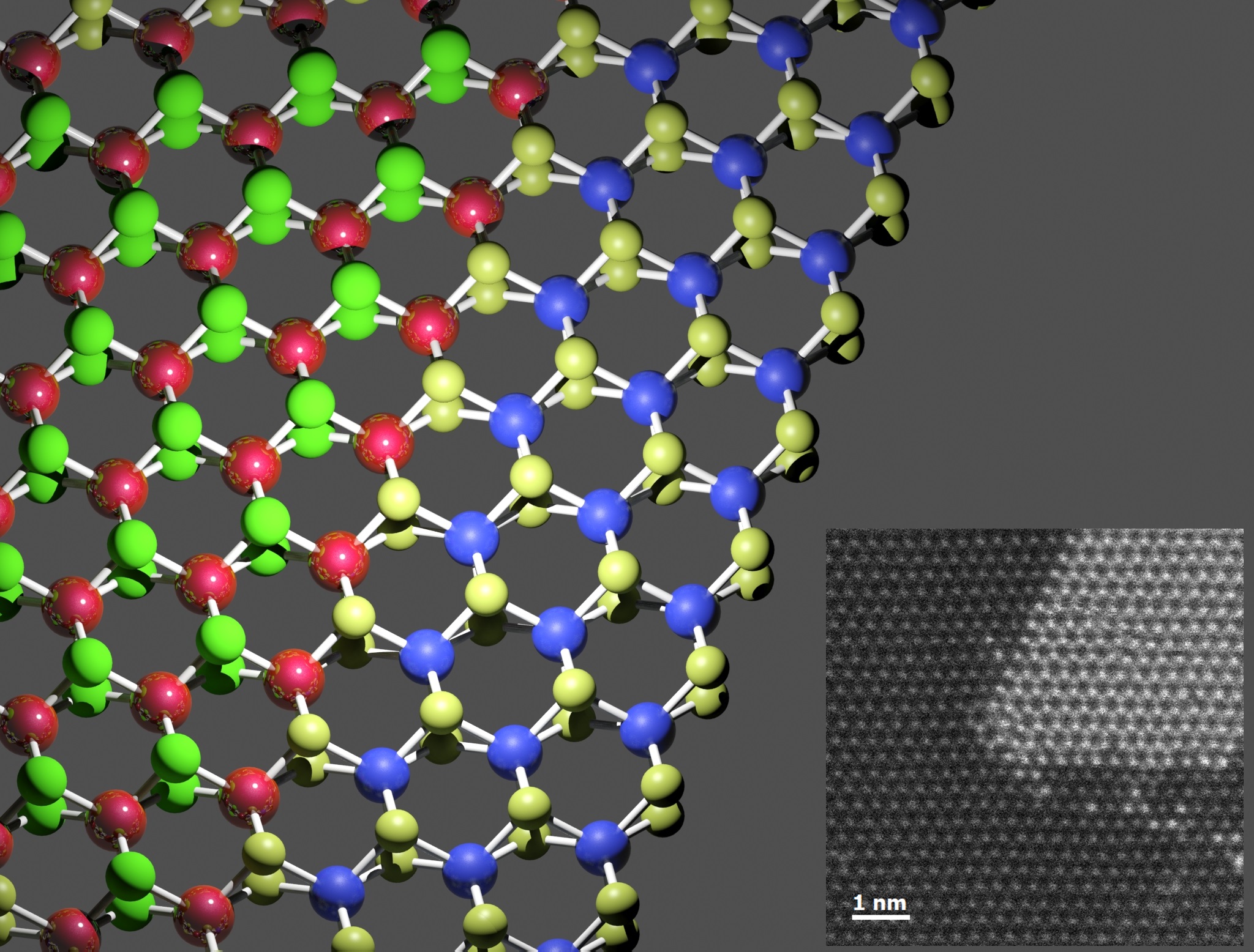
Heterostructures of 2D materials formed by vertical stacking have been realized recently via transfer of their exfoliated flakes, where their properties are dominated by the stacking orientation and strength of interlayer coupling. The method to determine valence band and conduction band alignment for various TMD materials is proposed [4]. Another very attractive structure is the lateral heterostructure, where the atomically sharp p-n junction exhibits diode properties and a large strain exhibits at the junction region which offers tenability in electronic structures. The direct growth of such lateral heterostructures is shown below (Figure 1) [5]. These unique 2D heterostructures have abundant implications for many potential applications.
TMD materials are also promising materials for post-Si electronics, where their ultra-thin body structure may be able to serve for 5 nm technology nodes [6] and a 10 nm channel length of transistor based on MoS2 few layers is demonstrated [7]. 
Fig. 1 Lateral heterostructure of MoS2and WSe2monolayers References [1] Y.-H. Lee et al. Adv. Mater. 24, 2320 (2012) [2] M. Chhowalla et al. Nature Chem. 5, 263-275 (2013) [3] C.-H. Chen et al. Adv. Mater. 26,4838 (2014) [4] M.-H. Chiu et al. Nature Comm. 6, 7666 (2015) [5] M.-Y. Li et al. Science 349, 524 (2015) [6] M.C. Chen et al. IEDM (2015) [7] K.H. Li et al VLSI (2016) |
